Smart textiles, wearables, IoT and digitalization are major drivers for printed electronics. High throughput deposition requirements demanding industry proved coating metrology, for applications such as:
Antennas
Various smart tags such as such as radio-frequency identification (RFID) tags
Sensors
Display and visual effects
(Inter)connection solutions
OPV
Batteries
Data Storage
Testing
Sheet resistance
Line resistance
Conductivity
Thickness
Homogeneity
Area weight
Drying status
Applications
Deposition process control
Tempering process control
Drying status control
Quality control
Substrates
Plastics
Glass
Ultra-thin glass
Foil
Process
S2S
R2R
Environment
In-vacuo and ex-vacuo
In-situ and ex-situ
Inline and offline
Wet and dry
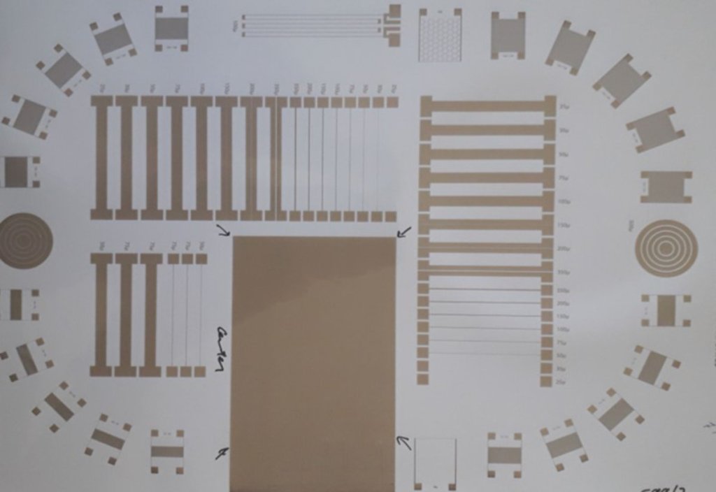
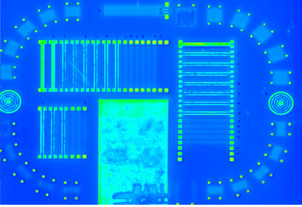
What Can You Expect From Eddy Current Imaging? Photo Image vs Eddy Current Image